gnangle wrote:Ebeam-What kind of plates are you scanning onto?
If you mean the SEM images on my site, these are all digital straight off the microscope. They are captured by scanning a focused electron beam pixel by pixel and collecting secondary electrons at each point.
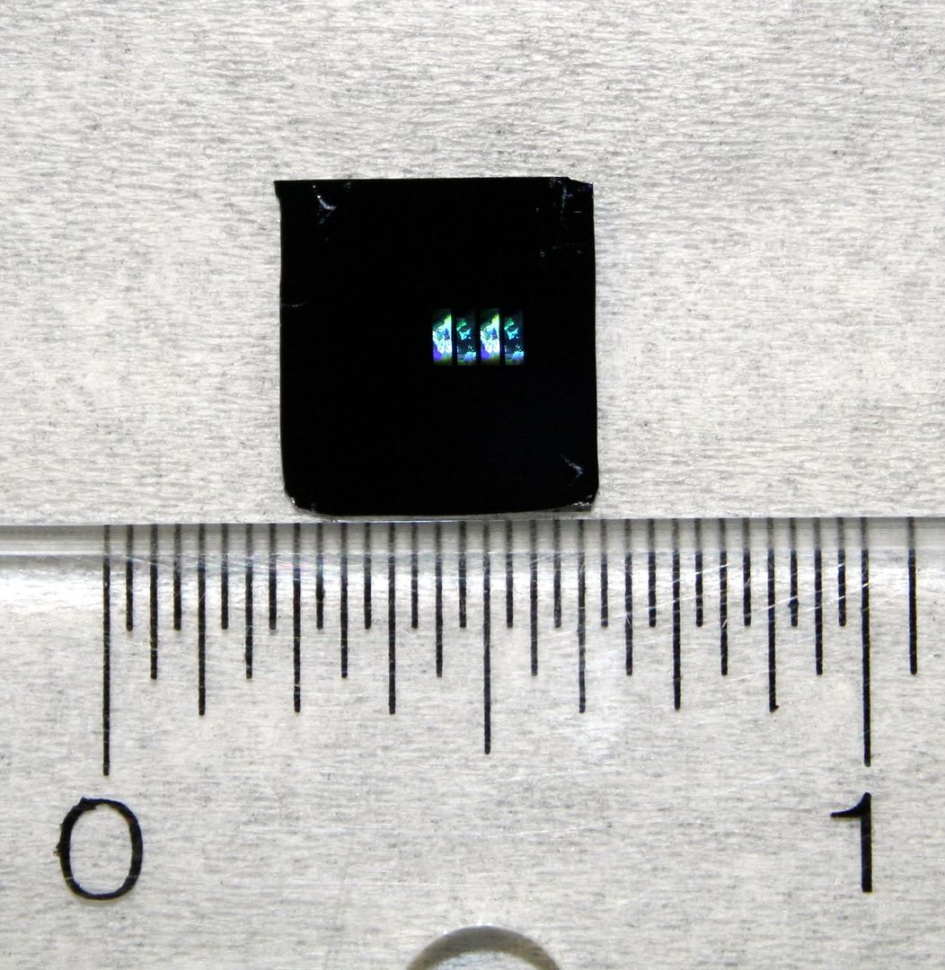
For the ultraminiature prints, I use a pretty standard electron beam lithography process, but it is certainly different that traditional lithography. I start with a highly polished single crystal silicon substrate and spin coat that with a very thin film of a poly-methyl methacrylate (PMMA) resist. I then use a computer to take control of the focused electron beam in the SEM and expose lines in the resist according to a CAD file I've designed. The electron beam breaks bonds in the PMMA, rendering it soluble in certain weak organic solvents. This exposed region developed by dissolving the exposed regions, leaving trenches in the resist layer. This is where I'm stopping for these prints as I like the irridescent quality of the image. You get different colors in the print due to optical interference effects in the thin film. In a typical process, though, you'd deposit a thin layer of some other material (say a metal) in the trenches and remove the rest of the resist layer, leaving patterned metal on the surface. I may do this for some future stuff. I'm thinking about putting carbon film down first as a dull background (the silicon is very shiny) and then putting gold patterns on top.